


Printable Thin-Film Transistors
Transistors are key micro-/nano-scale components of nearly all types of electronic circuits, where they realize the electronic functions needed for computing, sensing, and communications. The advent of printable semiconductors—such as organic semiconductors, amorphous metal-oxide semiconductors, and carbon nanotubes—has ushered in the new era of large-area electronics (LAE). At the heart of LAE are transistors made with nm-thick films of semiconducting materials—i.e., thin-film transistors (TFTs)—that can be deposited through facile methods onto low-cost, flexible plastic substrates. This enables the fabrication of TFTs with unique form factors, which is highly attractive to address emerging application areas (such as the Internet of Things) that require lightweight, flexible, and point-of-use electronics.
In addition to serving as the unit cells of large-area electronics, TFTs are complex physical systems in their own right, and can serve as a powerful testbed to study the physics of how charge carriers are transported within a given semiconductor. Therefore, by characterizing the electrical properties of a TFT under diverse conditions (e.g., at variable temperature, under illumination, under a magnetic field), it becomes possible to gain microscopic insight into the workings of the semiconductor the TFT is made of. Crucially, charge transport in TFTs occurs at the interface between a semiconducting thin film and a dielectric, and also involves the transfer of charges between such semiconductor and the metal electrodes it is in contact with. Therefore, TFTs also provide insight into the electronic properties of the corresponding interfaces, in terms of charge injection/confinement, trapping, and electronic disorder. By enabling the study of the charge transport and electronic properties of emerging semiconductors and their interfaces with metals and dielectrics, TFTs are therefore a formidable physics lab in the small scale.
Prof. Pecunia has extensively investigated organic, amorphous metal-oxide and carbon-nanotube-network TFTs. For example, he has demonstrated the well-conditioned charge confinement at the interface between polymer dielectrics and amorphous metal-oxide-semiconductors, establishing their wide compatibility for high-performance TFTs. Other important contributions concern the impact of trapping effects, minority carrier injection, and energetic disorder in organic TFTs, and the demonstration of solution-processible TFTs and circuits thereof with cutting-edge performance at reduced voltages.
Through material and process development as well as physical modelling, the Pecunia Research Group seeks to deliver new insights into the workings of TFTs based on emerging printable semiconductors. A key focus area concerns their charge transport and device physics at reduced electric field, as relevant to low-voltage, low-power TFT operation. Building on these insights, the Pecunia group also pursues the application of novel materials and device physics concepts for the integration of high-performance TFT electronics.
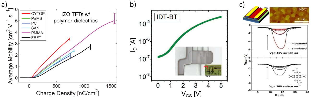
a) Demonstration of the wide compatibility of solution-process IZO with polymer dielectrics for high-performance n-channel TFTs (10.1002/adma.201503812).
b) Demonstration of high-performance low-voltage p-channel TFTs based on a solution-processed polymer semiconductor with small-molecule additives (10.1002/adma.201606938).
c) Characterisation of minority-carrier transport in a TFT based on a solution-processed organic semiconductor via Scanning Kelvin Probe Microscopy (10.1002/adma.201503812).
Representative Publications
L. Portilla*, J. Zhao†, Y. Wang, L. Sun, F. Li, M. Robin, M. Wei, Z. Cui, L. G. Occhipinti†, T. D. Anthopoulos†, V. Pecunia†*, Ambipolar Deep-Subthreshold Printed-Carbon-Nanotube Transistors for Ultralow-Voltage and Ultralow-Power Electronics, ACS Nano, 14, 10, 14036–14046, 2020. DOI: 10.1021/acsnano.0c06619
V. Pecunia†*, M. Fattori, S. Abdinia, E. Cantatore, H. Sirringhaus, Organic and Amorphous-Metal-Oxide Flexible Analogue Electronics, Cambridge University Press, Cambridge, UK, 2018. ISBN: 9781108458191, DOI: 10.1017/9781108559034
V. Pecunia†*, M. Nikolka*, A. Sou, I. Nasrallah, A. Y. Amin, I. McCulloch, H. Sirringhaus†, Trap Healing for High-Performance Low-Voltage Polymer Transistors and Solution-Based Analog Amplifiers on Foil, Advanced Materials, 29, 1606938, 2017. DOI: 10.1002/adma.201606938
Y. Hu*, V. Pecunia*, L. Jiang, C. Di, X. Gao, H. Sirringhaus†, Scanning Kelvin Probe Microscopy Investigation of the Role of Minority Carriers on the Switching Characteristics of Organic Field-Effect Transistors, Advanced Materials, 28, 4713–4719, 2016. DOI: 10.1002/adma.201503812
V. Pecunia, K. Banger, A. Sou, H. Sirringhaus†, Solution-Based Self-Aligned Hybrid Organic/Metal-Oxide Complementary Logic with Megahertz Operation, Organic Electronics, 21, 177–183, 2015. DOI: 10.1016/j.orgel.2015.03.004
V. Pecunia, K. Banger, H. Sirringhaus†, High-Performance Solution-Processed Amorphous-Oxide-Semiconductor TFTs with Organic Polymeric Gate Dielectrics, Advanced Electronic Materials, 1, 1400024, 2015. DOI: 10.1002/aelm.201400024
D. Venkateshvaran*, M. Nikolka*, A. Sadhanala, V. Lemaur, M. Zelazny, M. Kepa, M. Hurhangee, A. J. Kronemeijer, V. Pecunia, I. Nasrallah, I. Romanov, K. Broch, I. McCulloch, D. Emin, Y. Olivier, J. Cornil, D. Beljonne, H. Sirringhaus†, Approaching Disorder-Free Transport in High-Mobility Conjugated Polymers, Nature, 515, 384–388, 2014. DOI: 10.1038/nature13854